Think of diodes, and what comes to mind? That little flashing light on your phone charger? The infrared "eyes" on the front of the remote control? These are common applications of diodes in everyday life. As the basic component of an electronic circuit, a diode is like a "checkpoint" on a one-way street, allowing current to pass in only one direction (rectification). This seemingly simple function plays a key role in countless electronic devices.
In fact, the potential of diodes goes far beyond that. Professor Sun Haiting of the University of Science and Technology of China's iGaN Lab research group, Academician Liu Sheng of Wuhan University and his team have recently developed a multi-functional photodiode, which will raise the application prospect of diodes to a new height.

This article appeared as a cover article in Nature Electronics (photo source: Ref. 1)
"Super diode", heart or PN junction
This new multifunctional diode can not only be rectified like an ordinary diode, but also emit light like a light-emitting diode (LED), but also has the ability of photoelectric detection and logical calculation, really can be described as "three birds with one stone"! The realization of multiple functions in a single diode was previously unimaginable.
At the heart of this "super diode" is a gallium nitride based PN junction. As we all know, the PN junction is the "heart" of the diode, which is composed of two types of P-type and N-type semiconductors. When a positive voltage is added to both ends of the PN junction, electrons and holes will meet at the junction, resulting in a "recombination", which generates a current and makes the circuit open.
If this recombination process releases photons, the PN junction becomes a light-emitting diode, which converts electrical energy into light energy. Gallium nitride is a naturally suitable material for leds.


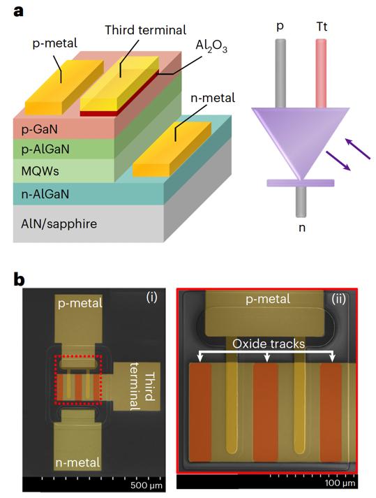
Diagram of the new diode (picture source: Reference 1)
By applying different voltages and adjusting the contact between the electrode and the p region, the carrier concentration in the PN junction region can be controlled, and then the luminous intensity and detection sensitivity of the device can be adjusted. Even better, the two regulatory signals can also simulate the input of the logic gate, so that the diode has the ability to perform logical operations.
See here, perhaps many readers have been confused, began to play back, don't worry, we will use everyone can understand the language, to give you the above words "translation" again.
"Stage" upgraded "Studio Center"
Super diodes have unique capabilities
In the traditional gallium nitride LED, the PN junction is like a "two-person stage", where the electrons in the n region and the holes in the p region meet and compound, and at the same time release photons, which are macrochemically manifested as a bright light.
The rhythm of this "dance" is mainly controlled by the voltage applied at both ends of the PN junction. The higher the voltage, the faster the electrons and holes "dance" and the greater the intensity of the light. But aside from adjusting the brightness, the "stage" doesn't seem to do much else.
The innovative design of Chinese researchers has given this "stage" a new ability. They added a separate third electrode above the P-zone. This electrode, like a "stage manager," can provide additional control over the dancers without affecting the PN knot's "performance."
Specifically, when a negative voltage is applied to the third electrode, it acts like a "vacuum cleaner" that can attract holes near the P-zone. The absence of holes, like fewer dancers on the stage, decreases the concentration of holes throughout the P-zone.
The change of the concentration of holes, which are the majority carriers in the P-region, will significantly affect the electrical properties of the PN junction. The decrease of hole concentration means that the conductivity of the p region becomes worse, the resistance of the PN junction increases, the probability of electrons and holes "meeting" decreases, and the luminous intensity will be weakened. Conversely, if a positive voltage is applied to the third electrode, more holes will be pushed towards the P-region, enhancing the luminescence of the PN junction.
Although adjusting the third electrode has a similar effect to adjusting the overall voltage, its regulation effect is more accurate and the energy loss is lower.
This is not all, the addition of the third electrode, so that it has a new application in photoelectric detection. When the diode works in reverse bias, the electric field inside the PN junction can separate the photogenerated electron-hole pair, generate photocurrent, and realize the detection of optical signal. The third electrode can change the intensity of the electric field in the PN junction by adjusting the hole concentration in the P-region, and then affect the size of the photocurrent. This is equivalent to a "zoom lens" that can adjust the photoelectric response sensitivity of the diode as needed.
What is even more amazing is that when the third electrode and the PN junction are considered as a whole, the device can actually simulate logical operations! Imagine that we can regard the voltage applied to both ends of the PN junction as an input signal, the voltage of the third electrode as another input signal, and the current output of the diode as a logical result.
By cleverly designing the circuit and adjusting the high and low levels of the two input signals, the diode can perform basic logical operations such as "and" or "no". This is equivalent to upgrading a simple "stage" into a multi-functional "studio center"!
Future development of the "super diode"
Of course, there are still many challenges to overcome before this technology can be applied, such as further optimizing device performance and improving the reliability and consistency of the manufacturing process. But there is no doubt that the advent of this multifunctional gallium nitride diode indicates that a more wonderful photoelectric world is quietly coming.
In this world, light, detection, and computing are no longer distinct, but perfectly integrated and closely coordinated in a single device. We have reason to believe that this breakthrough research results will certainly bring revolutionary changes to the future lighting, display, communication, computing and other fields.
Single device, multiple functions. This is not only a technological innovation, but also represents a new way of thinking. The "three-in-one" gallium nitride diode tells us that as long as the clever design and cross-border integration, a seemingly ordinary device can also release extraordinary potential. This also tells us that whether in scientific research or in other fields, breaking the inherent boundaries and daring to explore and innovate can always bring unexpected surprises.
reference
[1]A three-terminal light emitting and detecting diode, Muhammad Hunain Memon, Huabin Yu, Yuanmin Luo, Yang Kang, Wei Chen, Dong Li, Dongyang Luo, Shudan Xiao, Chengjie Zuo, Chen Gong, Chao Shen, Lan Fu, Boon S. Ooi, Sheng Liu & Haiding Sun
[2] Wu Changfeng. Used in optical communication and optical computing, China's first innovative field-effect regulation photodiode in the world
Planning and production
Produced by science popularization in China
Author Guo Fei, Yantai University
Producer of China Science Expo
Excerpt from: COPP China